


1. Introduction
With the development of 3D integrated packaging, through-silicon TSV has become one of the most promising technologies in 3D stacking packages [1-2]. Advanced TSV technology through the via and micro-bump achieves the vertical electrical connection between vertical stacks. It can also achieve the requirements of 3D heterogeneous integration of SiP, high-speed broadband, small size, and high performance.
TSV three-dimensional integrated devices with internal defects will gradually be failed by thermal mechanical stress, electrical stress, and other stresses, which will greatly affect TSV three-dimensional device reliability [3-4]. Ranganathan et al. [5] studied the influence of a fan-shaped interface generated by the Bosch etching process on TSV thermal stress. Koseski et al. [6]tested, modeled, and analyzed the stresses introduced by TSV with tungsten filling. Lau et al. [7] studied different spacing, different filling materials (copper and aluminum), and the thermal conductivity efficiency of different deep and wide ratio TSV chips.Chukwudi et al. [8] conducted a thermal cycling test on TSV and obtained the failure problems of void, crack, and oxidation in TSV under the condition of thermal cycling. Frank et al. [9] analyzed the reliability of TSV interconnecting for two technologies.
As a new interconnect technology, TSV technology faces many process difficulties and challenges [10-11]. The reliability has not been fully studied and guaranteed [12]. Identifying defects and analyzing the failure mechanism play important roles in the optimization and improvement of the design, production, and use of TSV 3D integrated devices [13-19].
In this paper, the microscopic physical analysis of boundary layers of TSVs with different shapes and aspect ratios are carried out. The via drilling process quality and the uniformity of the boundary layers are evaluated. The physical mechanism of the formation of various process defects and the possible failure impact are analyzed. Finally, the corresponding improvement measures are put forward according to the failure reasons.
2. Through Silicon Via Technology
By making vias on the silicon wafer and filling conductive material inside, TSV technology achieves vertical conduction between the chip and chip combined with bumps. Compared with traditional gold wire bonding, the advantage of TSV is that it saves the three-dimensional volume occupied by the external conductor. TSV technology can make a microelectronics chip package achieve the most compact connection and the smallest three-dimensional size. In addition, due to a reduction in the length of the connection lines between the chips, the interconnect delay is greatly reduced, and thereby the operation speed is increased. Due to the reduction of the interconnect resistance, the circuit power consumption is also greatly reduced. TSV technology can achieve heterogeneous integration by stacking different technologies and functions of logic chip, memory, MEMS, etc., as a system. There are many significant advantages for heterogeneous integration in terms of cost, performance, and time to market. TSV technology has the potential to improve 3D packaging. In the mainstream device design and production process, TSV interconnect technology will become inevitable. TSV is recognized as a fourth-generation interconnect technology following wire bonding (WB), tape automated bonding (TAB), and flip-chip (FC). Figure 1 shows the development of electronic packaging in these four stages.
Figure 1.
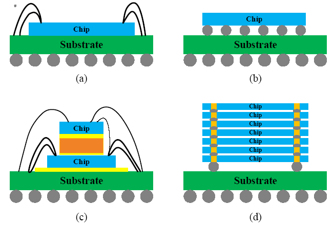
Figure 1.
Electronic packaging development stages: (a) wire bonding circuit; (b) flip chip circuit; (c) wire bonding three-dimensional integrated circuit;(d) TSV three-dimensional integrated circuit
3. Typical Process Defects and Failure Mechanismsof TSV
3.1. Void
Void defects are mainly generated in the filling process of TSV. The filling voids of the metal may cause an increase in the TSV interconnect resistance, a change in the performance of the device, and even an open failure of the circuit.
Incomplete filling is the most common problem in TSV processes [20]. In the process of electroplating Cu, the plating current density plays a crucial role. According to previous studies, when the current density continues to increase, the Cu plating rate also increases. The copper-filled growth mechanism is grown from the sidewall to the middle. Therefore, with an increase in the current density, the rapid increase in the plating rate leads to the closing with copper at the opening of via and voids formation at the bottom of the via.
Due to the shelling effect caused in the etching process, the via wall is not flat and the wetting is bad, which is another key reason for the formation of TSV filling voids. Poor wetting of the via can also cause serious interceptive defects of the plated metal layer. Uneven deposition of the seed layer also creates voids.
In addition, bubbles at the bottom of the via prevent the bottom of the hole from filling completely. Therefore, an effective way to avoid voids is to take measures to remove the bubbles at the bottom of the via before plating. The vacuum pretreatment method can effectively improve the TSV electroplating effect, so that the copper filling rate can be close to 100%.
If the voids are located within the insulating layer along the sidewall of the TSV, this will result in shortage or leakage between the TSV and the substrate.
3.2. Protrusion
After plating copper, redundant copper on the wafer surface needs to be removed by chemical mechanical polishing (CMP). Then, annealing follows. Due to the mismatch of the coefficient of thermal expansion (CTE) between Cu and Si, great thermal-mechanical stress is generated in TSV by the large temperature change before and after annealing. Due to the constraint of the surrounding Si substrate, Cu can only vertically expand outward in order to release the internal stress, which is called protrusion [21]. High temperature annealing also can cause lattice defects because of grain growth, as shown in Figure 2.
Figure 2.
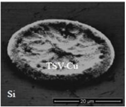
Figure 2.
Protrusion morphology of TSV-Cu during thermal cycling
Protrusion occurs in the annealing process, so the protrusion is influenced by different annealing conditions. It is shown that the annealing temperature is an important influence factor for protrusion [22]. The higher the annealing temperature, the more obvious the protrusion. In addition, the annealing time and TSV diameter, depth, spacing, and other parameters also have a certain role on the formation of protrusion.
Protrusion is an expression form of stress release. It will impact the reliability of the TSV device. On the one hand, the circuit around TSV can be extruded to failure by protrusion of TSV-Cu [23]. On the other hand, the structure around TSV can be pulled by protrusion of TSV-Cu, which will cause the metal interconnect layer to break (e.g. BEOL layer) [24].
3.3. Fracture and Delamination
Fracture and delamination are other major defects of TSV devices under high temperature processes, as shown in Figure 3. At present, in the typical process of TSV manufacturing, the material filled with vias as the conductor is mainly copper. Since the CTE among the filled Cu, Si substrate and the SiO2insulating layer do not match with each other [25], significant thermo-mechanical stresses will be generated inside TSV in the manufacturing process. Under thermo-mechanical stress, TSV and micro-bumps mayfracture, and micro-bumps may undergo delamination with TSV or bonding pads. Fracture and delamination may change the electrical properties of TSV devices, such as by increasing interconnection resistance.
Figure 3.
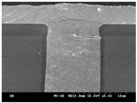
Figure 3.
Propagation of crack along the Top-M1-TSV interface after thermal cycles
4. Experiment and Analysis
4.1. Sample Introduction
The TSV sample chip had a total of $24\times 20$ vias. The left $12\times 20$ vias were square. The right $12\times 20$ vias were circular. The diameter or side length of each series of vias from left to right was decreased in turn, and it was always the same from top to bottom, as shown in Figure 4.
Figure 4.
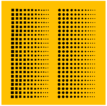
Figure 4.
Appearance of TSV sample surface
The first three process steps were completed including via drilling, isolation/buffer layer preparation, and Cu seed layer deposition. The boundary layers of the via are shown in Figure 5. Via filling, CMP, chip thinning, and bonding with other chips had not been completed.
Figure 5.
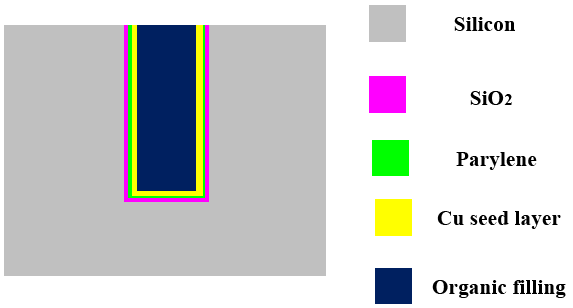
Figure 5.
TSV sample boundary layer material schematic
The depths of all the vias were almost the same, about 110 ~ 120$\text{ }\!\!\mu\!\!\text{ m}\text{.}$ The diameter or side length ranged from 15$\text{ }\!\!\mu\!\!\text{ m}$ to 95$\text{ }\!\!\mu\!\!\text{ m}\text{.}$ And the aspect ratio (AR) ranged from 1:1 to 5:1.
A series of vias on the chip should be defined before the experiment. Square vias by side length from large to small were named S1, S2, S3, L, S12. Circle vias by diameter from large to small were named C1, C2, C3, L , C12.
4.2. Via Drilling Process Quality Analysis
To evaluate via drilling process quality, cross section analysis was performed on the sample. As shown in Figure 6, the series of silicon vias were narrow at the top and wide at the bottom.
Figure 6.
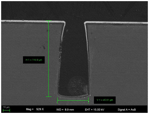
Figure 6.
Typical via cross section
Further analysis found that the larger the aspect ratio, the greater the difference between the top and bottom via diameter or side length, as shown in Figure 7. The red points represent the percentage of square vias side length difference between the top and the bottom. The green points represent the percentage of circle vias diameter difference between the top and the bottom. For the C12 silicon, the bottom via diameter was 27% more than the top.
Figure 7.
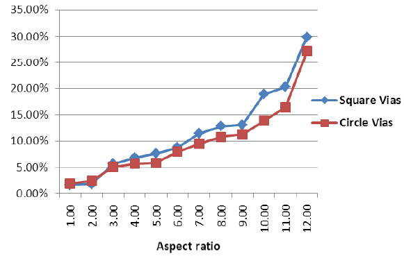
Figure 7.
Curves of via diameter or side length difference between the top and the bottom with aspect ratio
Vias drilling of the sample was done using Bosch etching, a deep reaction-ion etching processthat can form high aspect ratio features. By adjusting the ratio of the shielding gas C4F8 and the etching gas SF6, the shape of the vias could be changed. When the gases ratio was properly adjusted, vertical silicon vias were obtained, as shown in Figure 8(a). When the shielding gases ratio was larger, inverted trapezoidal silicon vias were obtained, as shown in Figure 8(b). When the etching gases ratio was larger, positive trapezoidal silicon vias were obtained, as shown in Figure 8(c). When the shielding gases were not used, oval vias were obtained, as shown in Figure 8(d).
Figure 8.
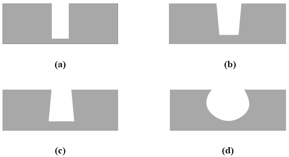
Figure 8.
Silicon vias of various shapes: (a) vertical; (b) inverted trapezoidal; (c) positive trapezoidal; (d) oval
Obviously, the etching gases ratio was larger in the drilling process for this sample, so the vias were positive trapezoidal. These positive trapezoidal vias would cause the silicon via closing in advance at the top in the next filling process, so the silicon via could not be filled completely, as shown in Figure 9.
Figure 9.
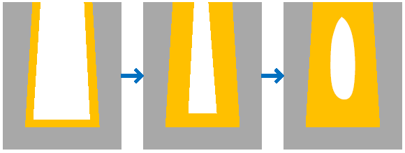
Figure 9.
Silicon via closing in advance at the top
4.3. Boundary Layers Quality Analysis
In order to evaluate boundary layer quality, 15 measurement points were taken on the vias sidewall to measure the thickness for each boundary layer, as shown in Figure 10.
Figure 10.
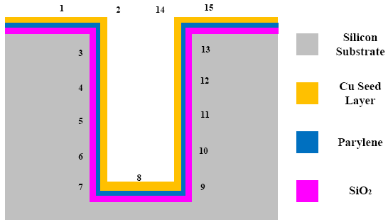
Figure 10.
Measurement points for each boundary layer
As shown in Figure 10, there are several important points that need to be noted. The measurement point 1 and the measurement point 15 recorded the thickness of the boundary layers on the wafer surface. The measurement points 2 and 14 recorded the thickness of the boundary layers at the top corner. The measurement point 7 and the measurement point 9 recorded the thickness of the boundary layers at the bottom corner. The measurement point 8 recorded the thickness of the boundary layers in the center of the bottom. S3 was selected as an example, and it had a width of about 80$\text{ }\!\!\mu\!\!\text{ m,}$ depth of about 120$\text{ }\!\!\mu\!\!\text{ m,}$ and aspect ratio of 1.5:1. The specific data is shown in Table 1.
Table 1. Thickness data of the boundary layers of S3
| Point | Cu seed layer($\text{ }\!\!\mu\!\!\text{ m}$) | Parylene layer($\text{ }\!\!\mu\!\!\text{ m}$) | SiO2 layer($\text{ }\!\!\mu\!\!\text{ m}$) |
|---|---|---|---|
| Point 1 | 2.89 | 1.13 | 2.30 |
| Point 2 | 2.34 | 0.99 | 1.94 |
| Point 3 | 1.56 | 0.85 | 1.18 |
| Point 4 | 1.27 | 1.02 | 1.00 |
| Point 5 | 0.47 | 0.99 | 0.39 |
| Point 6 | 0.68 | 0.97 | 0.33 |
| Point 7 | 0.80 | 0.76 | 0.36 |
| Point 8 | 0.71 | 0.86 | 0.42 |
| Point 9 | 1.11 | 0.71 | 0.37 |
| Point 10 | 0.38 | 1.17 | 0.52 |
| Point 11 | 0.76 | 1.12 | 0.85 |
| Point 12 | 0.77 | 1.33 | 1.20 |
| Point 13 | 0.99 | 0.85 | 1.67 |
| Point 14 | 1.85 | 1.09 | 2.06 |
| Point 15 | 2.99 | 1.21 | 2.12 |
| Average value | 1.30 | 1.00 | 1.11 |
| Mean square error | 0.82 | 0.17 | 0.71 |
From the data above, the average thickness value of the copper seed layer was 1.30$\text{ }\!\!\mu\!\!\text{ m}$ and the mean square error was 0.82$\text{ }\!\!\mu\!\!\text{ m}\text{.}$ The thickest point was 2.99$\text{ }\!\!\mu\!\!\text{ m,}$ and the thinnest point was only 0.38$\text{ }\!\!\mu\!\!\text{ m}\text{.}$ The uniformity of the copper seed layer was very poor. It was easy to fail at the thinnest point. The average thickness value of the parylene layer was 1um, and the mean square error was 0.17$\text{ }\!\!\mu\!\!\text{ m}\text{.}$ The values measured from each measurement point were basically offset by 1$\text{ }\!\!\mu\!\!\text{ m}\text{.}$ The parylene layer was more uniform. The average thickness value of the silicon dioxide layer was 1.11$\text{ }\!\!\mu\!\!\text{ m,}$ and the mean square error was 0.71$\text{ }\!\!\mu\!\!\text{ m}\text{.}$ The thickness of the silicon dioxide layer decreased as the depth of the silicon via increased. The thickest point was 2.3$\text{ }\!\!\mu\!\!\text{ m,}$ and the thinnest point was only 0.33$\text{ }\!\!\mu\!\!\text{ m}\text{.}$ The uniformity of the silicon dioxide layer was poor as well.
Figure 11.
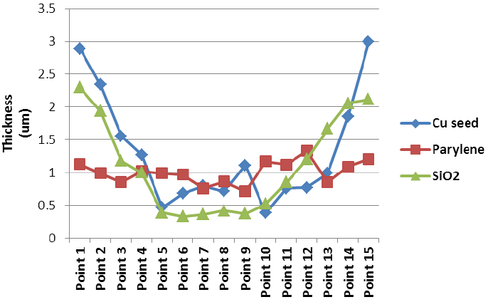
Figure 11.
Thickness change line chart of boundary layers
From the above chart, the copper seed layer at the top was thicker than the bottom. The copper seed layers were made by magnetron sputtering, a physical vapor deposition (PVD) method. The copper plasma ionized by argon glow discharge was composed of charged copper ions and neutral copper ions. Neutral copper ion flow is isotropic, so it was easier to accumulate in the upper part of the silicon via. Only the charged copper ion flow, under the guidance of the current, could more easily access the deeper parts of the silicon via. There were less copper ions entering the bottom of the silicon vias, so the thickness of the copper seed layers decreased with depth.
Because the copper seed layers at the top were thicker, the silicon via may have closed in advance at the top in the filling process. In other words, there would be voids at the bottom.
In terms of the above method, the thickness of the copper seed layer of the six vias S3, S5, S8, C3, C5, and C8 was measured, as shown in Table 2.
Table 2. Thickness data of the copper seed layer of different vias
| Via No. | S3 | S5 | S8 | C3 | C5 | C8 |
|---|---|---|---|---|---|---|
| Diameter/Side length($\text{ }\!\!\mu\!\!\text{ m}$) | 79.6 | 71.1 | 48.6 | 78.6 | 67.6 | 46.2 |
| Depth($\text{ }\!\!\mu\!\!\text{ m}$) | 120.0 | 122.8 | 115.3 | 115.0 | 115.5 | 111.2 |
| Aspect ratio | 1.5 | 1.7 | 2.3 | 1.5 | 1.7 | 2.4 |
| Average value($\text{ }\!\!\mu\!\!\text{ m}$) | 1.31 | 1.26 | 1.07 | 1.12 | 1.07 | 0.98 |
| Mean square error($\text{ }\!\!\mu\!\!\text{ m}$) | 0.823 | 0.855 | 0.870 | 0.823 | 0.945 | 0.995 |
As shown in Figure 12, the average thickness value of the copper seed layers decreased with an increasing aspect ratio. However, the mean square error of the copper seed layers increased. Therefore, the uniformity of the copper seed layers deteriorated with an increasing aspect ratio. In addition, the copper seed layers of the square silicon vias were thicker and more homogeneous than the circle silicon vias.
Figure 12.
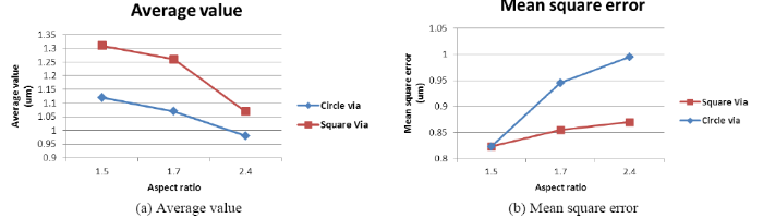
Figure 12.
Thickness change line chart of copper seed layer with aspect ratio
4.4. Boundary Layers Defect
As shown in Figure 13, the TSV boundary was divided into three layers. The first layer was the copper seed layer for electroplating copper. The second layer was the buffer layer of parylene. The third layer was the insulating layer of SiO2.
Figure 13.
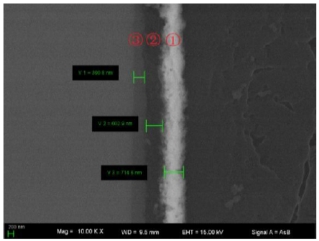
Figure 13.
SEM analysis of TSV boundary layers
Figure 14.
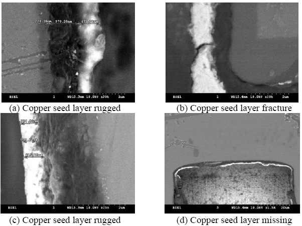
Figure 14.
Various defects of copper seed layer
The copper seed layer is better-proportioned and continuous, and there are fewer voids and cracks in the copper plating. That is, voids and cracks in the silicon vias are largely dependent on the flatness of the copper seed film. The roughness of the copper seed film is related to many parameters in the magnetron sputtering process, including bias voltage, silicon substrate temperature, plating time, and reaction chamber pressure.
As shown in Figure 15, if the surface of the copper seed layer is not flat and the thickness of the copper seed layer is not uniform, voids and cracks may occur at the thinnest location of the copper seed layer. This is because the copper seed layer at the thinnest location may dissolve and be lost in the electroplating process.
Figure 15.
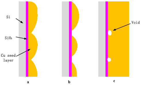
Figure 15.
Void formation process: (a) uneven seed layer; (b) the seed layer partially dissolved in plating solution; (c) the void appeared at the thinnest location of the copper seed layer
It was also found that the parylene layer was delaminated from the silicon dioxide layer, as shown in Figure 16 from SEM analysis. From EDS analysis, the main component of the filaments between the parylene layer and the silicon dioxide layer was parylene. It was speculated that delamination was produced by stress stretching due to the mismatch of thermal expansion coefficients of the parylene layer and the silicon dioxide layer.
Figure 16.
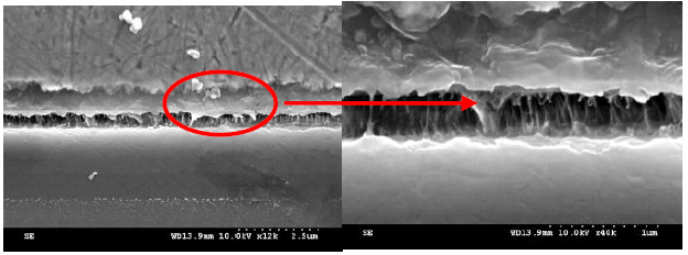
Figure 16.
Delamination between parylene layer and silicon dioxide layer
From the point of view of the technical process, if the silicon dioxide layer was not cleaned before, adhesion between the parylene layer and the silicon oxide layer would be poor. In addition, certain gases introduced in the actual process production, such as HF, will have a significant effect on the adhesion of the parylene and the silicon dioxide.
5. Results and Discussion
According to a series of experimental analysis on the TSV samples, it was found that there were several process defects:
$\cdot\$ The series of silicon vias were narrow at the top and wide at the bottom because the etching gases ratio was too large in the drilling process. These positive trapezoidal vias would cause the silicon via closing in advance at the top in next filling process, so the silicon via would not be filled completely.
$\cdot\$ Copper seed layers were uneven. The copper seed layer at the top was thicker than that at the bottom. The uniformity of the copper seed layers deteriorated with an increasing aspect ratio. In addition, the copper seed layers of square silicon vias were thicker and more homogeneous than those of circle silicon vias.
$\cdot\$ Fractured and missing copper seed layers were observed. Delamination between the parylene layer and the silicon dioxide layer was also observed.
According to the analysis of the production process and physical mechanism of defect formation, the following suggestions were put forward:
$\cdot\$ In the process of deep reaction-ion etching, the proportion of the etching gas SF6 would be appropriately reduced, and the proportion of the shielding gas C4F8 would be increased.
$\cdot\$ In the process of magnetron sputtering of copper seed film, the process parameters would be adjusted appropriately, including increasing the bias power, increasing the temperature of the silicon substrate, and setting the appropriate argon gas pressure.
$\cdot\$ New technological means for the deposition of copper seed layer could be adopted, such as double-sided plating.
$\cdot\$ The surface of the silicon dioxide would be cleaned before parylene deposit to improve the adhesion between the parylene layer and the silicon oxide layer
6. Conclusions
TSV three-dimensional integrated devices, which are involved in a variety of new structures, new materials, and new technology, havebrought a series of new reliability issues. As an important physical connection and electrical connection between the chips, TSV’s reliability is undoubtedly the key to determine the reliability of TSV three-dimensional integrated devices. The via drilling process quality and the uniformity of the boundary layers havedirect and significant impacts on the performance of silicon vias.
Reference
“3D Copper TSV Integration, Testing and Reliability, ”
DOI:10.1109/IEDM.2011.6131504
URL
[Cited within: 1]

Node-agnostic Cu TSVs integrated with high-K/metal gate and embedded DRAM were used in functional 3D modules. Thermal cycling and stress results show no degradation of TSV or BEOL structures, and device and functional data indicate that there is no significant impact from TSV processing and/or proximity.
“New Three-Dimensional Integration Technology using Chip-to-Wafer Bonding to Achieve Ultimate Super-Chip Integration, ”
“Analysis of the Electrical Characteristics and Structure of Cu-Filled TSV with Thermal Shock Test, ”
DOI:10.1007/s13391-013-3260-6
URL
[Cited within: 1]

The electrical characteristics and failure of a Through-Silicon Via (TSV) were investigated using a thermal shock test. The electrical characteristics, such as resistance ( R ), self-inductance ( L s ), self-capacitance ( C s ), and mutual capacitance ( C m ), were extracted using a T-equivalent circuit. A cross section of the Cu-filled via was observed by field emission-scanning electron microscopy and the electrical characteristics were measured using a commercial Agilent E4980A LCR Meter. The experimental results revealed R , L s , C s , and C m values of 3.2 m , 29.3 pH, 12 fF, and 0.42 pF, respectively. C m occurred between the charge-holding TSVs, which changed from 0.42 pF to 0.26 pF due to a permittivity transition of the Cu ion drift. After 1, 000 cycles of a thermal shock test, cracks were observed between the opening and around the side of the TSV and Si wafer due to mismatch of the coefficient of thermal expansion between the Cu-plug and Si substrate.
“Interfacial Effects During Thermal Cycling of Cu-Filled Through-Silicon Vias (TSV),”
DOI:10.1007/s11664-011-1726-6
URL
[Cited within: 1]
Large shear stresses may develop at interfaces between dissimilar materials during thermal excursions when there is a significant difference in their coefficients of thermal expansion. The shear stress may cause interfaces to slide via diffusional process, thereby accommodating the relative dimensional changes between the two materials. This phenomenon presents a significant reliability issue in three-dimensional (3-D) interconnect structures involving through-silicon vias (TSVs), which are subjected not only to continuous thermal cycling but also to large electric current densities during service. This paper reports experimental evidence of interfacial sliding between Cu and Si in Cu-filled TSVs during thermal cycling conditions, and in the presence of electric current. Two different thermal cycling conditions were used: (i) small Delta T thermal cycling (-25degC to 135degC) and (ii) large Delta T thermal cycling (25degC to 425degC). Prior to thermal cycling, a few Cu-filled TSV samples were annealed for 30 min at 425degC. Cu intruded inside Si in nonannealed samples during small Delta T thermal cycling, where as protrusion of Cu relative to Si occurred during all other thermal excursions. Application of electric current biased the net displacement of the Cu in the direction of electron flow, leading to enhanced protrusion (or intrusion) of Cu relative to the thermal cycling only (i.e., without electric current) condition. A simple one-dimensional analytical model and associated numerical simulations are utilized to rationalize the experimental observations.
“Influence of Bosch Etch Process on Electrical Isolation of TSV Structures, ”
DOI:10.1109/TCPMT.2011.2160395
URL
[Cited within: 1]
Bosch process is widely used in the fabrication of through silicon via (TSV) holes for 3-D integrated circuit and 3-D Packaging applications mainly due to its high silicon etch rate and selectivity to mask. However, the adverse impact on the electrical performance of the TSV due to the sidewall scallops or wavy profile due to the cyclical nature of the Bosch process has not been thoroughly investigated. This paper therefore focuses on the impact of sidewall scallops on the inter-via electrical leakage performance. Based on finite element analysis, this paper describes that the high stress concentration on the dielectric and barrier layers at the sharp scallops can potentially contribute to barrier failure. It is demonstrated that by smoothening the sidewalls of the TSV, the thermo-mechanical stresses on the dielectric and tantalum barrier is significantly reduced. A test vehicle is designed and fabricated with different geometry of deep silicon vias to study the impact of sidewall profile smoothening for different copper diffusion barrier stacks. It is experimentally demonstrated that the inter-via electrical leakage current can be reduced by almost three orders of magnitude when the sidewall roughness is reduced or replaced by a smoother sidewall. It is also indicated that it is sufficient to smoothen the initial few micrometers of the TSV depth by using a non-Bosch etch process. It is concluded that the Bosch etch process can still be used, with all its merits of high etch rate and high etch selectivity, by tailoring a short initial etch step to smoothen the top sidewalls to minimize the adverse effects of the sidewall scallops.
“Micro-Scale Measurement and Modeling of Stress in Silicon Surrounding a Tungsten-Filled Through-Silicon Via, ”
DOI:10.1063/1.3644971
URL
[Cited within: 1]
The stress in silicon surrounding a tungsten-filled through-silicon via (TSV) is measured using confocal Raman microscopy line scans across the TSV both before and after etch removal of an oxide stack used as a mask to define the TSV during fabrication. Stress in the silicon arose in response to both athermal deposition and thermal expansion mismatch effects. The complex three-dimensional stress and strain field in silicon surrounding the TSV is modeled using finite element analysis, taking into account both athermal and thermal effects and the elastic anisotropy of silicon. Comparison of the measurements and model results shows that no one component of the stress tensor correlates with the Raman peak shift generated by the deformed silicon. An analysis is developed to predict the Raman shift in deformed silicon that takes into account all the components of the stress or strain tensor; the results of the model are then used as inputs to the analysis for direct comparison with measured peak shifts as a function of distance from the TSV. Good agreement between the measured and predicted peak shifts is obtained for the case of the intact oxide stack. A discrepancy between the measured and predicted shifts was observed adjacent to the TSV with the oxide stack removed; further modeling suggests the discrepancy is explained by the formation of a small void at the TSV-silicon interface during etching. The combined measurement-modeling approach serves to both validate the model, in this case for TSV design, and to extend the measurement capability of confocal Raman microscopy to complex stress fields.
“Effects of TSVs (Through-Silicon Vias) on Thermal Performances of 3D IC Integration System-in-Package (SiP),”
DOI:10.1016/j.microrel.2012.04.002
URL
[Cited within: 1]
Thermal performances of 3D IC integration system-in-package (SiP) with TSV (through silicon via) interposer/chip are investigated based on heat-transfer and CFD (computational fluid dynamic) analyses. Emphases are placed on the determination of (1) the equivalent thermal conductivity of interposers/chips with various copper-filled, aluminum-filled, and polymer w/o filler filled TSV diameters, pitches, and aspect ratios, (2) the junction temperature and thermal resistance of 3D IC SiP with various TSV interposers, (3) the junction temperature and thermal resistance of 3D stacking of up to 8 TSV memory chips, and (4) the effect of thickness of the TSV chip on its hot spot temperature. Useful design charts and guidelines are provided for engineering practice convenient.
“A Detailed Failure Analysis Examination of the Effect of Thermal Cycling on Cu TSV Reliability, ”
DOI:10.1109/TED.2013.2291297
URL
[Cited within: 1]
In this paper, the reliability of through-silicon via (TSV) daisy chains under thermal cycling conditions was examined. The electrical resistance of TSV daisy chains was found to increase with the number of thermal cycles, due to thermally induced damage leading to the formation and growth of defects. The contributions of each identified damage type to the change in the electrical resistance of the TSV chain were evaluated by electrical modeling. Thermo-mechanical modeling showed a good correlation between the observed damage locations and the simulated stress-concentration regions of the TSV.
“Reliability of TSV Interconnects: Electromigration, Thermal Cycling, and Impact on above Metal Level Dielectric, ”
DOI:10.1016/j.microrel.2012.06.021
URL
[Cited within: 1]
In this paper, reliability of Through Silicon via (TSV) interconnects is analyzed for two technologies. First part presents an exhaustive analysis of Cu TSV-last approach of 2μm diameter and 15μm of depth. Thermal cycling and electromigration stresses are performed on dedicated devices. Thermal cycling is revealed to induce only defects on non-mature processes. Electromigration induces voids in adjacent metal level, right at TSV interface. Moreover, the expected lifetime benefit by increasing line thickness does not occur due to increasing dispersion of voiding mechanism. Second part covers reliability of Cu TSV-middle technology, of 10μm diameter and 80μm depth, with thermal cycling, BEoL dielectric breakdown, and electromigration study. Thermal cycling is assessed on two designs: isolated and dense TSV patterns. Dielectric breakdown tests underline an impact of TSV on the reliability of metal level dielectrics right above TSV. Electromigration reveal similar degradation mechanism and kinetic as on TSV-last approach.
“The 3-D Interconnect Technology Landscape, ”
DOI:10.1109/MDAT.2016.2544837
URL
[Cited within: 1]
This overview article sheds light into the diverse notions and terms associated with 3-D circuits. It categorizes and classifies the various technologies/techniques and helps the experienced researcher as well as a newcomer to find an orientation in the complex 3-D landscape.
Al-Hashimi, “Online Fault Tolerance Technique for TSV-Based 3-D-IC, ”
“Reliability Challenges Related to TSV Integration and 3-D Stacking, ”
DOI:10.1109/MDAT.2015.2501302
URL
[Cited within: 1]
This article identifies four major reliability challenges related to TSV-based 3-D integrated circuits and their solutions that are being developed at imec.
“Reliability Evaluation of Copper (Cu) Through-Silicon Vias (TSV) Barrier and Dielectric Liner by Electrical Characterization and Physical Failure Analysis (PFA),”
in
DOI:10.1109/ECTC.2017.77
URL
[Cited within: 1]
The motivation behind this study is to detect barrier and dielectric liner degradation in a copper (Cu) through-silicon via (TSV) structure. The integrity of titanium (Ti) barrier and silicon dioxide (SiO2) dielectric liner are evaluated via a non-destructive electrical characterization method after being subjected to different stress tests such as high temperature storage (HTS), temperature cycling (TC) and electrical biasing. The various different stresses were either performed independently, or performed as a combination stress with electrical bias for comparison. After performing the respective stresses, capacitance-voltage (C-V) and current density-electric field (J-E) characteristics were analyzed to identify differences in its electrical characteristics. Degradation of the barrier liner may result in the migration of Cu from the Cu via into the dielectric liner. This is identified by changes observed in the inversion capacitance, as reflected in the C-V curve. Physical failure analysis (PFA) was performed on degraded structures and verified the presence of Cu in the dielectric due to barrier degradation as detected by the electrical measurement. It is suggested that barrier degradation leading to the migration of Cu into the dielectric liner can be associated to material and structural integrity which is dependent on the stress conditions. This understanding is useful in the reliability assessment of Cu TSV structures under various stress conditions, making it appropriate for future TSV degradation studies.
“Experimental Insights into Thermal Dissipation in TSV-based 3-D Integrated Circuits, ”
DOI:10.1109/MDAT.2015.2506678
URL
This article describes heat dissipation challenges in 3-D ICs; using two case studies, it also presents insights and design guidelines for 3-D thermal management.
“Failure Analysis Work Flow for Electrical Shorts in Triple Stacked 3D TSV Daisy Chains, ”
in
“Assembly Technology Development and Failure Analysis for Three-Dimensional Integrated Circuit Integration with Ultra-Thin Chip Stacking, ”
DOI:10.1016/j.mee.2016.01.040
URL
61This study presents a process for wafer handling and robust assembly for thin chip stacking.61A pre-molding technology is used to achieve extra-thin chip thickness down to 10μm.61Testing vehicle is fabricated to demonstrate the possibility of proposed approach.61A simulation methodology is adopted to find the stress-induced failure of vehicles.61Effects of underfill flexibility and die thickness of proposed framework are considered.
“High Resolution 3D X-Ray Microscopy for Streamlined Failure Analysis Workflow, ”
in
DOI:10.1109/IPFA.2016.7564285
URL
High resolution 3D X-ray microscopy is a powerful non-destructive technology to inspect internal failure of IC packages. Here we present a correlative workflow by combining thermal emission microscopy, high resolution 3D X-ray microscopy and dual-beam focused ion beam microscopy to analyze a failed FCBGA package.
“Failure Analysis on the Mechanical Property of Through-Silicon Vias Interface using a Cohesive Zone Model, ”
in
DOI:10.1109/ICEPT.2016.7583372
URL
Through Silicon Via(TSVs) technology is one of the most prominent feature in future microelectronic devices packaging. Since TSVs contain the interfaces of heterogeneous materials that have high CTE mismatch, and would hence produce large thermal stresses under temperature loading, often leading to mechanical failure. A failure stress mathematical model is established and the algorithm of mathematical model is prepared by using subroutine and fracture failure modeling of Cu/SiO2 interface in TSV using finite element method (FEM) with cohesive zone model as well as stiffness degradation evaluation criterion was employed. Numerical simulation results show that large thermal stresses induced by the unique feature of TSV structure and the high mismatch of CTE between silicon substrate, dielectric layer and copper core, would lead to Cu/SiO2 interface delamination and the failure mode of the interface is shear stress predominantly. The phase angle at the tip of interfacial crack is almost 80 degrees when the interface was about to crack and then it will decrease as the crack grows gradually. However, the value of phase angle is always more than 45 degrees. Additionally, the fracture analysis to the damage process of interfacial crack under mixed-mode loading has been derived based on power law of energy criterion. It is noted that the temperature cracking of the interface is reduced and the crack propagation of Cu/SiO2 will difficult as the fracture energy of cohesive elements increases.
“An Overview of Scanning Acoustic Microscope, a Reliable Method for Non-Destructive Failure Analysis of Microelectronic Components, ”
in
DOI:10.1109/eurosime.2015.7103077
URL
[Cited within: 1]
In a highly competitive and demanding microelectronics market, reliable non-destructive methods for quality control and failure analysis of electronic components are highly demanded. Any robust non-destructive method should be capable of dealing with the complexity of miniaturized assemblies such as chip-scale packages and 3D IC stacks. Scanning acoustic microscopy (SAM) is indeed one the best non-destructive tools for failure analysis purposes. It is also a useful technique for imaging the morphology, location and size distribution of defects in different microelectronics components. SAM can detect delaminations at sub-micron thicknesses. It is also one of the only available techniques capable of efficiently evaluating popcorning in PBGA's and is a also useful device to detect sub-micron air gaps. SAM can also be used to measure the thickness of an internal layer of material. Overall, SAM is an efficient tool for evaluating such a wide range of different defects in printed circuit boards, underfills, BGAs, wire bonds, discrete components, and wafers. In SAM a focused sound is directed from a transducer at a small point on a target object, as is schematically shown here. Sound, hitting a defect, inhomogeneity or a boundary inside material, is partly scatted and will be detected. The transducer transforms the reflected sound pulses into electromagnetic pulses which are displayed as pixels with defined gray values thereby creating an image. This article aims at giving an overview of scanning acoustic microscope (SAM) and explaining its operating principles and its limitations. A few examples are also given for further clarification.
“Non-Destructive Testing of a High Dense Small Dimension Through Silicon Via (TSV) Array Structures by using 3D X-Ray Computed Tomography Method (CT Scan),”
in
DOI:10.1109/EPTC.2010.5702683
URL
[Cited within: 1]
In the present study, high density TSV structures have been designed and fabricated with different diameter and depths, ranging from 2 to 60 m and 50 to 100 m respectively. The ratios of TSV diameter to space between TSVs are 1:2, 1:3 and 1:4. Inspection of TSV structures at each processing step is very crucial to proceed to next step. 3D X-ray CT scan analysis has been employed to inspect TSV wafers at different processing steps. Detailed 3D X-ray CT scan analysis has been carried out on 20, 50 and 60 um TSV array structures. Using this method, it is possible to observe defect shape, size and distribution by conducting the virtual cross-section at desired location. Based on the detailed online failure analysis, TSV process development parameter are being fine-tuned and optimized.
“Study on Cu Protrusion of Through-Silicon Via, ”
DOI:10.1109/TCPMT.2013.2252955
URL
[Cited within: 1]
The through-silicon via (TSV) approach is essential for 3-D integrated circuit (3-DIC) packaging technology. TSV fabrication process, however, is still facing several challenges. One of the widely known challenges is via protrusion. Annealing a TSV wafer puts the copper (Cu) TSVs under high stress and may form a protrusion where the Cu is forced out of the blind TSV. This phenomenon occurs because the large mismatch in the coefficient of thermal expansion between Cu via and silicon (Si) surrounding it. Cu protrusion can lead to crack or delamination of the back-end-of-line, thus, it is a risky threat to the metal layer interconnect. Experiments are conducted to characterize the protrusion using several techniques. Scanning electron microscopes and atomic force microscopes are used to observe the protrusion shape and measure the height. An electron backscatter diffraction technique is implemented to study the grain size distribution and evolution inside Cu vias. For the experiment, arrays of 5-mu m TSVs are fabricated and annealed in nitrogen gas environment in different temperatures. In this paper, finite element analysis (FEA) is carried out to study the Cu protrusion under different annealing conditions. Correlation between numerical results and experimental data is then carried out. Based on the verified FEA methodology, several parametric studies are then conducted, including the effect of via diameter, depth, pitch, annealing temperature, and duration on Cu protrusion and TSV stress. The simulation results help to understand and solve the key problem in TSV fabrication process and reliability challenge.
“Cu Pumping in TSVs: Effect of Pre-CMP Thermal Budget, ”
DOI:10.1016/j.microrel.2011.06.003
URL
[Cited within: 1]
When Cu ‘Through-Silicon-Vias’ (TSVs) are exposed to high temperatures as typically encountered during the back-end of line (BEOL) processing, the higher coefficient of thermal expansion (CTE) of Cu forces it to expand more than Si. This causes compressive stress in the confined Cu inside the TSV. This stress can partly be released near the top of the TSV, by out-of-plane expansion of the Cu, the so-called ‘Cu pumping’. It can severely damage the BEOL layers. In this paper the effect of a pre-CMP thermal budget (temperature and time) on Cu pumping is studied for various Cu chemistries and TSV aspect ratios. It is shown that to suppress Cu pumping a pre-CMP anneal is required that is either very long or at a temperature very close to the maximum temperature used in the BEOL processing.
“Impact of Post-Plating Anneal and Through-Silicon Via Dimensions on Cu Pumping, ”
in
DOI:10.1109/ECTC.2013.6575633
URL
[Cited within: 1]
Irreversible extrusion of Cu from through-silicon vias (TSVs) during high-temperature processing steps presents an important potential back-end-of-line (BEOL) reliability issue. Commonly this reliability risk is mitigated by introducing an anneal after Cu plating for TSV fill. This paper presents the impact of the post-plating anneal temperature and time on residual Cu pumping during a sinter for 20 min at 420 C, for two different TSV dimensions. Using optical profilometry, in total ~ 4000 TSVs were measured, allowing detailed statistical analysis. Within one sample the Cu pumping values were found to be log normally distributed, implying an intrinsically large spread. Lower residual Cu pumping values were found in TSVs annealed at higher temperatures and for longer times, with the sinter conditions of 20 min at 420 C confirmed as optimal post-plating anneal conditions. The larger TSVs showed more pumping in the average TSV, but at the tail of the distribution the Cu pumping behavior was the same as for the smaller TSVs. This implies that the impact of Cu pumping on BEOL reliability is identical for both sets of TSV dimensions, suggesting that the impact of Cu pumping on BEOL reliability is not necessarily reduced by reducing TSV dimensions.
“A View on Annealing Behavior of Cu-Filled Through-Silicon Vias (TSV),”
“Thermal Expansion Behavior of Through-Silicon-Via Structures in Three-Dimensional Microelectronic Packaging, ”
DOI:10.1016/j.microrel.2011.11.001
URL
[Cited within: 1]
Thermo-mechanical reliability is an important issue for the development and deployment of the through-silicon-via (TSV) technology in three-dimensional (3D) microelectronic packaging. The mismatch in coefficient of thermal expansion (CTE) between the array of copper (Cu) lines and the surrounding silicon (Si), upon temperature variation, affects the overall thermal expansion behavior of the whole TSV structure itself and generates an internal stress state. In this work we use the finite element method to numerically study the effective in-plane CTE of the Si/Cu composite structure. A 3D unit-cell approach is undertaken, which takes into account uniformly distributed TSVs in the Si chip. Results of the temperature-dependent effective CTE can be used as model input for simulating larger-scale 3D packages where the Si/Cu TSV structure is treated as a homogeneous material. We also examine the evolution of stress and deformation fields, and identify potential reliability concerns associated with the thermal loading.
